Data Center Transition to CO-PACKAGED OPTICS (CPO) - FREE
The CPO (Co-Packaged Optics) is an emerging technology that integrates optical components directly into the chip package.
The chips that power AI models (GPUs) never work alone: they operate in massive clusters, continuously exchanging enormous amounts of data through light signals, far faster and more efficient than traditional copper cables.
Until now, though, the optical components managing that light were physically separate from the chip, like a USB drive plugged into a port. Every connector wastes energy and reduces speed. At the scale modern AI architectures require, so many of these modules are needed that the energy consumption becomes simply unsustainable.
CPO solves this by integrating the optical component directly into the chip package, eliminating the connector entirely. This results in:
- Reduced latency: Faster response times since the components are close together.
- Higher energy efficiency: Traditional modules consume more due to connectors and interfaces.
- Greater bandwidth density: Optical communications have a higher transmission capacity than copper cables.
Hyperscalers will need to source from an entire photonic supply chain. This means growth potential for the companies within it.
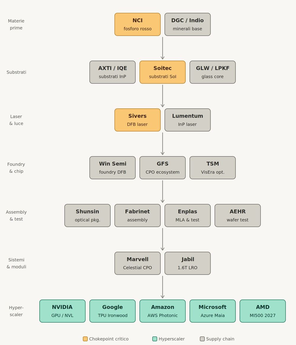
Photonics Supply Chain
The introduction of the CPO will require a new photonic supply chain that covers several key technological components. The chain is composed of different levels, as follows:
1. RAW MATERIALS
Raw materials are the starting physical point for the entire photonic supply chain. Without them, there would be no laser, substrate, or CPO. There are generally two types:
- Indium:
A rare metal almost exclusively extracted as a by-product of zinc smelting. It does not have dedicated mines and is recovered from zinc processing residues, making it inherently scarce and difficult to obtain quickly. The main global producers are China (which controls over 50% of the market), South Korea, Japan, and Canada. It is used to produce InP (Indium Phosphide) crystals, which are the substrates on which DFB lasers are grown, forming the core of the CPO (Chip-on-Board). - High-purity Red Phosphorus (6N/7N):
Phosphorus is the second ingredient of InP. "6N" indicates 99.9999% purity, while "7N" means even higher purity. This extreme purity is required because even the smallest impurities in the crystal can create defects that impair the optical efficiency of the laser. Phosphorus is abundant in nature, but refining it to such high purity is a complex industrial process that only a few companies in the world can carry out.
2. SUBSTRATES
Substrates are the base materials on which photonic components and chips are mounted.
- InP (Indium Phosphide) is an advanced semiconductor material used for high-speed photonic applications, such as lasers and optical modulators, due to its excellent light-handling properties and high transmission speeds. It's ideal for advanced systems but is complex and expensive to produce.
- SOI (Silicon on Insulator) uses a silicon substrate with an insulating layer that improves energy efficiency and reduces losses, allowing for photonic-electronic integration. It is cheaper and more scalable than InP but is suitable for lower transmission speeds.
3. LASERS AND LIGHT SOURCES
Lasers are the heart of optical transformation. They are used to generate coherent light, which can be modulated to carry information. Data bits are converted into light pulses by the laser, which are then transmitted through the optical fiber. The fiber guides the light using total internal reflection, reducing signal loss. The light can be modulated, with data bits represented as variations in the light flow (for example, varying intensity, phase, or frequency). Finally, when the signal reaches the end of the fiber, it is converted back into an electrical signal through a photodiode or optical detector.
4. FOUNDRY
A PIC (Photonic Integrated Circuit) is a chip that manipulates light instead of electrons. It contains components such as waveguides (which guide the light), modulators (which encode data onto the light), photodetectors (which convert light into electrical signals), and WDM multiplexers/demultiplexers (which separate channels at different wavelengths). In a CPO system, the PIC acts as a "bridge" between the optical and electronic worlds, integrating directly with the GPU or ASIC.
Photonics foundries are factories that produce these integrated photonic circuits, transforming base materials (such as wafers) into functional components that manipulate light.
5. ASSEMBLY, PACKAGING, AND TESTING
Assembly, packaging, and testing in CPO is a complex process that requires precise optical alignment at the nanometer level between components. Unlike traditional transceivers, the laser is directly coupled to the photonic chip, a process that requires specialized equipment and advanced expertise. Even a small misalignment increases losses, making this step a high-value-added process.
6. SYSTEMS AND MODULES
The systems and modules level integrates photonic components into complete systems, such as transceivers and CPO modules, ready for installation in data centers. The main distinction is between pluggable and CPO. Pluggable modules are flexible but have limits, such as losses caused by the connector. CPO eliminates the connector, integrating the optical module directly into the chip, reducing losses, energy consumption, and improving bandwidth. However, CPO production is complex. There are also intermediate LRO and LPO architectures, which are solutions without the full CPO integration but still utilize optical components.
7. HYPERSCALER
Hyperscalers are the end customers of the entire supply chain and determine the speed and scale of the technological supercycle. Their decisions influence the entire chain, including investments in infrastructure and architecture. CPO is inevitable for hyperscalers, as next-generation GPU clusters (e.g., NVIDIA Blackwell) require optical bandwidths in the terabit-per-second range to interconnect chips. Traditional 400G or 800G pluggable modules cannot handle this demand, resulting in unsustainable energy consumption. CPO solves the problem by reducing connectors, losses, and consumption, allowing AI clusters to scale beyond certain limits.
If one believes that AI is a true revolution, it could be decided to enter this supply chain.
There are more general levels, such as those of raw materials, which can also be used for other purposes (not just AI), and more specific levels, such as those of hyperscalers.
Le informazioni pubblicate da Daniele Cristaldi hanno esclusivamente scopo informativo e divulgativo. Nulla di quanto riportato costituisce consulenza finanziaria, sollecitazione all'investimento, né raccomandazione di acquisto o vendita di strumenti finanziari ai sensi del D.Lgs. 58/1998 (TUF) e della normativa MiFID II. Le analisi e le opinioni espresse riflettono unicamente il punto di vista personale dell'autore e non devono essere interpretate come garanzia di risultati futuri. Qualsiasi decisione di investimento è adottata dall'utente sotto la propria esclusiva responsabilità.